Samsung Develops World’s First 900-Layer V-NAND Prototype Chip

SammyGuru is reader-supported. We have affiliate and sponsored partnerships, so we may earn a commission when you buy through links on our site — at no extra cost to you. Learn more.
Samsung is once again stirring the pot in the industry as it pushes the limits of NAND flash technology. With AI workloads exploding and data demands going through the roof, memory makers are under pressure to deliver larger, faster, and more efficient storage. Now Samsung has developed a 900-layer-class V-NAND prototype.
Samsung moves closer to 1,000-layer NAND with 900-layer prototype chip
Needless to say, it marks a significant leap in storage technology. According to ETNews, the company achieved this using Cell Multi-Bonding, a method that connects two 450-layer cell stacks into a single structure. As a result, this enables higher density while keeping power consumption under control.
Scaling NAND to this level has introduced manufacturing challenges. Higher stacks can lead to wafer warping and alignment issues during production. Samsung addressed these problems with an improved Upper Chuck design and updated overlay correction technology. It also refined bitline and wordline structures to reduce chip size and improve power efficiency.
In the current market, SK Hynix leads in shipping high-layer NAND with its 321-layer products. Yangtze Memory Technologies Co. is also expanding quickly, moving toward 300-layer NAND with strong local support. Competition is increasing, especially as demand rises for AI and data-driven applications. Samsung is working on both fronts, preparing 400-layer NAND for production while advancing higher-layer research.
The 900-layer prototype is still in the research stage, but it shows how NAND scaling is evolving. Instead of relying only on single-stack designs, new bonding techniques are coming into the picture. Samsung’s progress suggests that 1,000-layer NAND is achievable. However, it will take further development before it reaches mass production.

Written by
Abhinav AnandAbhinav Anand is the News Editor at SammyGuru and a technology journalist based in New Delhi. Before joining SammyGuru, he contributed to numerous outlets, including Android Headlines, ExtremeTech, The Mac Observer, Financial Express, Economic Times, iGeeksBlog, KnowTechie, PhonesWiki, SlashGear, and more. You can reach him at [email protected].

Follow us on Google Discover & set us as a preferred source in Google News
Share this Post
___________________________


New Blog Posts
___________________________
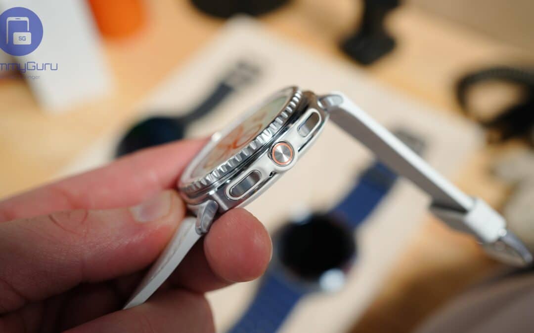
Miss the Rotating Bezel? Galaxy Watch 8 Classic Is Now Half Off
A deal that’s hard to ignore
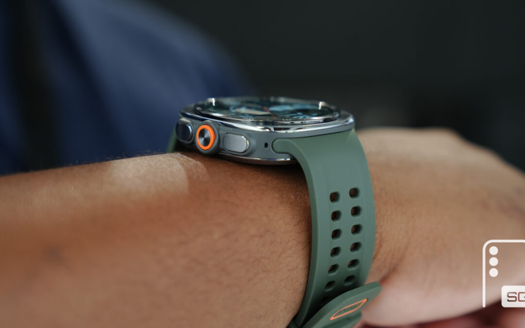
Samsung Could Benefit as Global Wearable Market Shrinks in 2026
Premium smartwatches are still growing, and that’s good news for Samsung
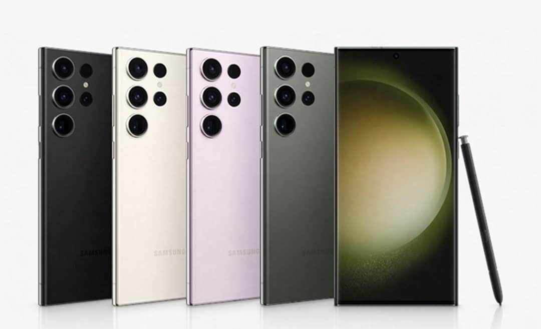
Galaxy S23 Gets July 2026 Update in More Regions, Galaxy A27 Gets First Update
Samsung has already begun One UI 9 testing for these models